


Berlin is the hub for photonics in Germany - Report from the Photonics Days Berlin Brandenburg 2018
Berlin is the hub for photonics in Germany
Report from the Photonics Days Berlin Brandenburg 2018
Exhibition in the Bunsensaal at WISTA Berlin Partner für Wirtschaft und Technologie GmbH / Photothek
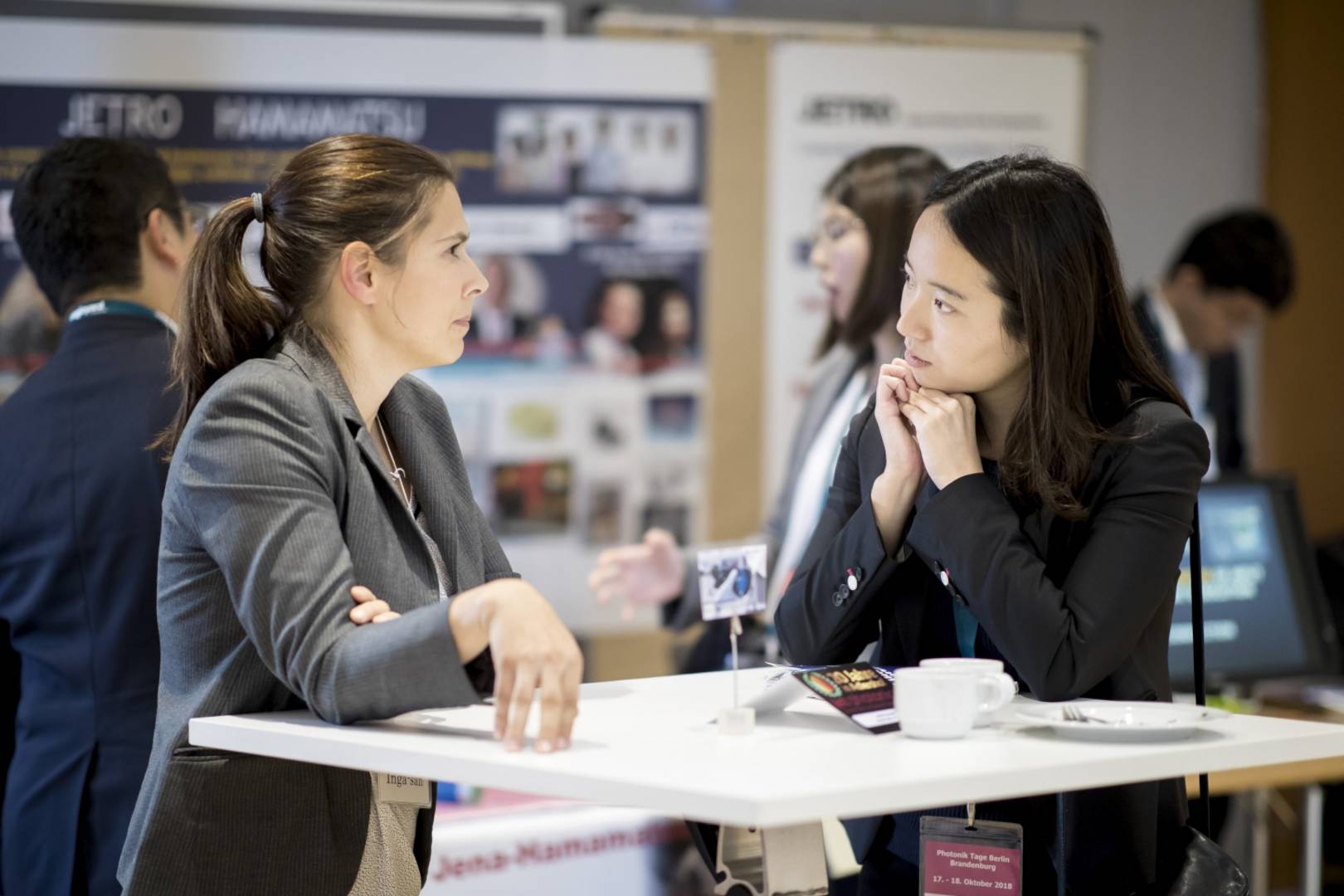
Over 600 visitors from all over the world came to the Photonics Days Berlin Brandenburg 2018. The topics covered almost all areas of applied photonics, from spectroscopy and solar energy to sensors for autonomous driving and quantum technologies. Start-ups, small and large companies as well as many scientists from Germany, the USA, Japan, Brazil, Israel and many European countries took part.
Many of the local photonics experts could be met at the Photonics Days Berlin Brandenburg on 17 and 18 October in Berlin Adlershof. More than 600 visitors from Germany and all over the world came to discuss topics from the full range of this key technology. The following table gives an initial overview of the variety of topics with the various lecture events.
The event with about 160 lectures and 55 exhibitors was organized by OptecBB e.V. with the support of Berlin Partner für Wirtschaft und Technologie GmbH, Wirtschaftsförderung Land Brandenburg GmbH and WISTA Management GmbH.
From LIDAR to Quantum Sensors: Insights into the Topic Spectrum
Peter Krause from FirstSensor AG moderated the workshop (Handlungsfeldkonferenz) on microsystems technology. As local spokesman of the field and president of the AMA Association for Sensor and Measurement Technology, he is always amazed how many companies in the region are working on and with sensors. With his lecture From sensor integration to sensor fusion he also pointed out a major trend: In topics such as sensors for autonomous driving, it is not only important to manufacture sensors small and inexpensive. In the future, different systems will also have to operate in a network or even on one chip (“sensor fusion”). At the same time, sensors will become more intelligent by carrying more functions with more software. For Krause this means: Sensor manufacturers must understand more about the applications.
Networking and intelligent technology are also hot topics for Dr. Henning Schröder (Fraunhofer IZM), who moderated the Photonics for Communication and Sensor Technology workshop (Handlungsfeldkonferenz). Photonics for Secure and High Speed Communication was this year's motto. Quantum communication is on the rise, but so is the further integration of optical components for networking sensors and systems. According to Schröder, Berlin-based companies are among the world leaders in assembly and connection technology.
At the evening reception, Prof. Dr. Martin Schell, head of the Fraunhofer Heinrich Hertz Institute HHI and spokesman for the regional Photonics Cluster in Berlin and Brandenburg, pointed out that many of the components for future quantum communication systems are being investigated and developed here in the region. To this end, the institutes in Berlin and Brandenburg are heavily involved in initiatives such as the German Microelectronics Research Factory (FMD) or the 650 million euro funding program for quantum technologies from the Federal Ministery for Education and Research (BMBF).
Welcome Reception by Prof. Dr. Martin Schell and Permanent Secretary of Senate for Economics, Energy and Public Enterprises Christian Rickerts Berlin Partner für Wirtschaft und Technologie GmbH / Photothek
Accordingly, the Berlin Quantum Optics Symposium: Metrology and Imaging was also an important part of the Photonics Days. Companies and research groups from all over Europe took the opportunity to present their projects and plans. Dr. Patrick Leisching from toptica AG in Munich, for example, presented an entire roadmap on how they intend to develop components and technologies for the various fields of application of quantum technologies.
In addition to telecommunications, materials processing is now a major area of application for laser technology. Dr. Arnold Mayer (Optech Consulting) showed in the workshop (Handlungsfeldkonferenz) Laser Technology that this market with a turnover of 17 billion dollars is currently experiencing a strong upswing: 28% growth last year and 5-10% in this year speak for the success of industrial laser technology worldwide. In the discussions in the industrial laser community, the focus is currently shifting from beam sources to applications and the necessary production technology. This was demonstrated both in the various presentations at the workshop and in the subsequent workshop of the Fraunhofer Institute for Production Systems and Design Technology IPK. Additive manufacturing is just one keyword for new trends that are now arriving in production. The concluding tour of the Fraunhofer IPK also provided important insights into new production methods.
Polyphotonics Workshops Berlin Partner für Wirtschaft und Technologie GmbH / Photothek
Networking works here locally and globally
While connecting systems were a big topic at the whole conference, connecting people were at least as important during the Photonics Days: People from various companies and institutes came together to talk about a wide variety of projects, across topics and countries. The forms of cooperation are plentiful and varied, and so were the opportunities at the Photonic Days to get to know new partners and new topics. For example, visitors to the Laser Technology workshop had a chance to learn something about the regional laser markets in Poland, Brazil and Japan from experts out of those countries.
An example of interdisciplinary thinking was the lecture Autonomous networked photonic sensor systems in precision farming - a wish list by Dr: Manuela Zude-Sasse from the Leibniz Institute for Agricultural Engineering and Bioeconomics ATB, where the potential (and needs) for cooperation with more distant research areas became obvious.
Networking at Photonic Days 2019 Berlin Partner für Wirtschaft und Technologie GmbH / Photothek
Some fascinating insights were delivered by start-ups and new settlements in several workshops. They gave prove how photonic technologies are gaining critical mass in the capital region. Professor Karsten König, for example, has just founded a branch of his company JenLab on the Adlershof campus: We will also bring our other branches to Berlin. Here we simply have the best infrastructure in Germany with long-standing partners on both the technical and clinical sides.” Berlin Adlershof is now home to around 100 small and medium-sized photonics companies.
New cluster report presented
The full range of photonics activities in the region is provided by the Cluster Report Optics & Photonics in the Capital Region Berlin Brandenburg. It was presented for the first time at the Photonics Days. Over 80 research institutions and over 200 companies contributed to this brochure. Visitors to the Photonics Days were able to get to know a selection of them in the two exhibition rooms with a total of 55 stands.
New Clusterreport presented by Dr. Frank Lerch, OpTecBB e. V. towards the permanent secretary Christian Rickerts Berlin Partner für Wirtschaft und Technologie GmbH / Photothek
The photonics industry in the capital region is developing excellently. Accordingly, Berlin is increasingly becoming a meeting place for photonics experts from all over the world. Carlos Lee, head of the European Photonics Industry Consortium EPIC, also sees it this way: Berlin is the hub for photonics in Germany, he says. After a start in spring 2018, he will hold his World Photonics Technology Summit 2019 again in Berlin.
The next Photonics Days Berlin Brandenburg are planned for the end of November 2019 in Potsdam.
This article was written by Andreas Thoss.